

Solder resist material forms the protective mask over a printed circuit board’s circuit pattern. It helps keep solder away from unintended areas during assembly and remains as a protective coating afterward. You will also encounter the term solder mask in discussions of this PCB surface layer.
Three separate questions often get mixed together: which material is specified, how it is applied, and how the required pattern is formed. Separating them makes a board specification easier to discuss. A coating method or a green surface photograph alone does not identify the complete material requirement.
What solder resist material does on a PCB
Taiyo’s manufacturer overview describes solder resist as an insulating ink that covers and protects the circuit pattern. Its stated roles include controlling where solder adheres and protecting covered circuitry from environmental influences such as dust and moisture.
The surface pattern matters as well as the material. Some areas are covered; intended contact areas remain open. The illustration shows that distinction without assigning a thickness, opening dimension or manufacturing tolerance.
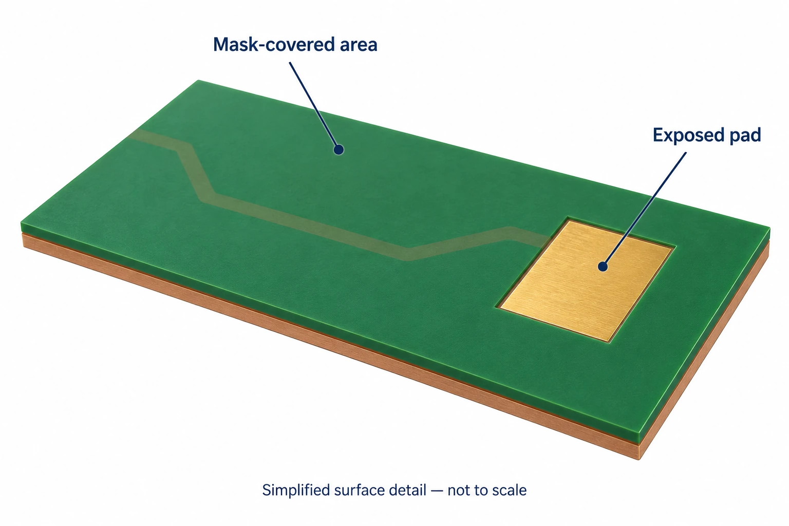
The protective role is a material-function description, not an electrical safety rating for a finished assembly. Suitability for a particular application needs evidence for the specified material, construction and conditions. Appearance alone cannot establish that suitability.
Material type and coating method are different descriptions
The manufacturer groups solder resists by film-forming method into alkaline-developable, UV-curable and thermally curable types. These descriptions concern how the resist is patterned or hardened. They should not be treated as a complete list of every formulation or product available.
The same manufacturer’s application overview separately describes screen printing, spray coating and curtain coating. Those terms describe ways of putting material onto a board. They answer a different question from the material’s film-formation category.
For example, saying “screen printed” identifies an application approach but leaves the exact grade and its processing requirements unresolved. Saying “UV curable” describes a hardening characteristic but does not, by itself, provide the complete coating and pattern specification.
| Description level | Examples or information | What it leaves unresolved |
|---|---|---|
| Film formation | Alkaline-developable, UV-curable, thermally curable | Exact grade and approved process conditions |
| Coating method | Screen print, spray coat, curtain coat | Material identity and final pattern |
| Pattern requirement | Covered areas and intended openings | Applicable drawing revision and acceptance details |
| Material specification | Manufacturer, grade and current supporting data | Whether the offered construction meets the application need |
How photoimageable pattern formation fits
The manufacturer’s photoimageable example describes applying resist, exposing it to light through a pattern and developing away unwanted portions. The resulting pattern leaves selected areas covered and others open. That explains the concept; it is not a ready-to-run process for another material.
A supplier’s published example may include particular preparation or curing conditions. Do not transfer those settings into a different grade or factory process without the applicable material guidance and process evaluation. A general explainer cannot establish a production window.
This is a useful distinction when reviewing a drawing comment such as “photoimageable mask.” The phrase tells you something about pattern formation, but a buyer still needs the exact material, drawing and process information relevant to the order.
Questions that make a supplier discussion more useful
The characteristics page notes that requirements vary with the board, coating method, assembly and testing processes, and final application. Rather than asking whether a material is simply “good,” identify the requirement the supplier needs to address.
Which grade is offered? Request the full material designation and current supporting document. If the quotation lists a broad family while the technical sheet covers several products, ask the supplier to connect the offered grade to the relevant data.
Which pattern is controlled? Identify the drawing or design-data revision governing covered areas and openings. A surface photograph is useful orientation, but it does not replace the controlled pattern requirement. Resolve inconsistent versions before treating a sample as representative.
Which process context was evaluated? Ask which coating and assembly context the evidence concerns. Keep the supplier’s process explanation attached to the material identity. If a proposed substitution changes that context, make the change visible for the responsible technical review.
What establishes acceptance? Distinguish a typical characteristic from an agreed acceptance criterion. Record the relevant requirement, the evidence supplied and any unanswered question. A tidy document pack is only useful when its contents relate to the board and material actually being purchased.
These questions form an original discussion aid, not a manufacturing instruction. They are especially useful when an offer contains familiar technical terms but does not yet connect them into a clear specification.
For the reader trying to identify solder resist, the essential distinction is simple: it is the PCB’s patterned protective mask. For the reader specifying it, the next step is to connect the grade, pattern, process context and evidence. This article does not establish that a particular Wanze product uses any named solder resist material.
References
- Taiyo: What is solder resist? — definition, roles and film-formation categories.
- Taiyo: Required characteristics — application-dependent material requirements.
- Taiyo: Application of solder resist — coating and photoimageable patterning concepts.